Skip to product information
1 of 2

Robocraze

CD4049 - Hex Inverting Buffer/Converter IC

CD4049 - Hex Inverting Buffer/Converter IC

Regular price Rs. 15
Regular price Rs. 19 Sale price Rs. 15
Sale Sold out 21% off Best Price Guaranteed
You save Rs. 4 | Free Shipping on Orders Above ₹ 499/-
Incl. GST (No Hidden Charges)
Currently, people are actively viewing.

BEST COUPON FOR YOU

FLAT ₹ 100/- OFF RC100

When you shop for ₹ 2500 or more.Applicable on Checkout.

*Coupons are not applicable on Original Boards and Kits

Submit your Bulk Enquiry Here

Contact form

  • Wide supply voltage range
  • Direct drive to 2 TTL loads at 5.0V over full temperature range
  • High source and sink current capability
  • Special input protection permits input voltages greater than VDD

CD4049 - Hex Inverting Buffer/Converter IC

The CD4x Series CD4049 hex buffers are monolithic complementary MOS (CMOS) integrated circuits constructed with N- and P-channel enhancement mode transistors. These devices feature logic-level conversion using only one supply voltage (VDD).

The input signal level can exceed the VDD supply voltage when these devices are used for logic-level conversions. These devices are intended for use as hex buffers, CMOS to DTL/TTL converters, or as CMOS current drivers, and at VDD=5.0V, they can drive directly two DTL/TTL loads over the full operating temperature range.

check out : CD4504 - Hex Voltage Level Shifter IC
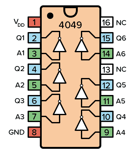
Pinout:

Pinout Of CD4049 IC
Pin Name Pin # Type Description
VDD 1 Power Supply Voltage (+3 to +15V)
GND 8 Power Ground (0V)
Q1-Q6 2, 4, 6, 10, 12, 15 Input Inputs to the inverters
A1-A6 3, 5, 7, 9, 11, 14 Output Outputs from the inverters
NC 13, 16 Not Connected

Applications:

  • CMOS hex inverter/buffer
  • CMOS to DTL/TTL hex converter
  • CMOS current "sink" or "source" driver
  • CMOS high-to-low logic level converter

Package Includes:

Selected qty of IC - CD4049

Specifications:

Part number CD4049
Technology Family CD4000
VCC (Min) (V) 3
VCC (Max) (V) 18
Channels (#) 6
Output type Push-Pull
Input Type Standard CMOS
ICC @ nom voltage (Max)(mA) 600
Features Standard speed (tpd > 50ns), Over-voltage tolerant inputs, Unbuffered
IOL (Max) (mA) 18
IOH (Max) (mA) -3.1
Rating See Data Sheet
Data rate (Mbps) 24
Package Group PDIP|16

Shipping & Returns

  • All orders confirmed before 3 pm IST are shipped on the
    same day, barring rare pickup delays on holidays or disturbances
  • Delivery time in Metro cities is 1-3 days, Others it is
    3-7 days. It varies based on location, reliant on courier services
  • Return window: 7 days from receipt unless stated
    otherwise. No refunds/replacements after
  • Returns only for non-working/damaged products are accepted
  • Initiate return requests to our customer service team via Support ticket or contact us at +91-8123057137
  • Refunds are processed within 3-4 working days post inspection and approval.

For more details, please check our Shipping and Return Policy

View full details

Found a better price?

Let us know!
We'll try to match the price for you

  • ⚡ Dispatched within 24 hours

  • 💰 Earn RC Coins on every purchase

  • 🚚 Free shipping on orders above Rs 500/-

  • 🛠️ Dedicated Technical Support Team

1 of 4

ADDITIONAL RESOURCES

1.What is CD4049?

  • The CD4049 is a hex inverting buffer/converter, which means it has six NOT gates (inverters) and a higher sink current than most logic gates. It has 16 pins, two of which are disabled. Because it can accept a higher input voltage than its supplied VDD voltage, this chip is frequently used for level shifting.

2.What is a NOT gate/Inverter?

  • A NOT gate (or inverter) is a logic gate that produces the inverse of what it receives. As a result, a 1 (HIGH) on the input results in a 0 (LOW) on the output.

3.How to Use the CD4049 in a Circuit?

  • To use the CD4049 in a circuit, a power supply voltage of 3 to 20V is required. Connect the chip's VDD and GND pins to the power supply. You can now use any of the six inverters by connecting something to the input and output pins.